In Module 10
Aufgaben
Introduction, structure and function of operational amplifiers
Modelling and characteristic variables

The previous module explained how single-stage and multi-stage transistor amplifiers can be used to amplify signals with low input amplitudes. These amplifier circuits were primarily used in measurement and control technology and, until the 1950s, were constructed discretely from electron tubes or transistors. The development of integrated circuits enabled the miniaturisation of circuits from the end of the 1960s onwards, thereby providing modular components for hardware development. This also applied to the differential amplifiers developed in the 1940s, which, due to their initially widespread use in analogue computers, are also referred to as operational amplifiers (from ‘operator’). This module covers the basics of operational amplifiers.
The following skills are to be acquired in this chapter:
Learning objectives: Operationsverstärker
The students can
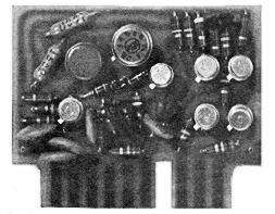
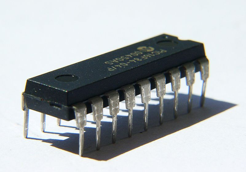
Operational amplifiers (also referred to as OPV or OpAmp for short) are characterised by the fact that they are designed as universal amplifiers and their function is largely determined by external circuitry. This means that the same component can be used to amplify voltages , perform arithmetic operations such as addition, subtraction or integration, and switch signals. Such operational amplifiers are indispensable in measurement and control technology, signal processing and signal shaping, for example. The following shows an operational amplifier constructed from discrete transistors and an integrated circuit. Due to the direct coupling of the amplifier stages, operational amplifiers can amplify DC and AC voltages and are therefore classified as DC voltage amplifiers.
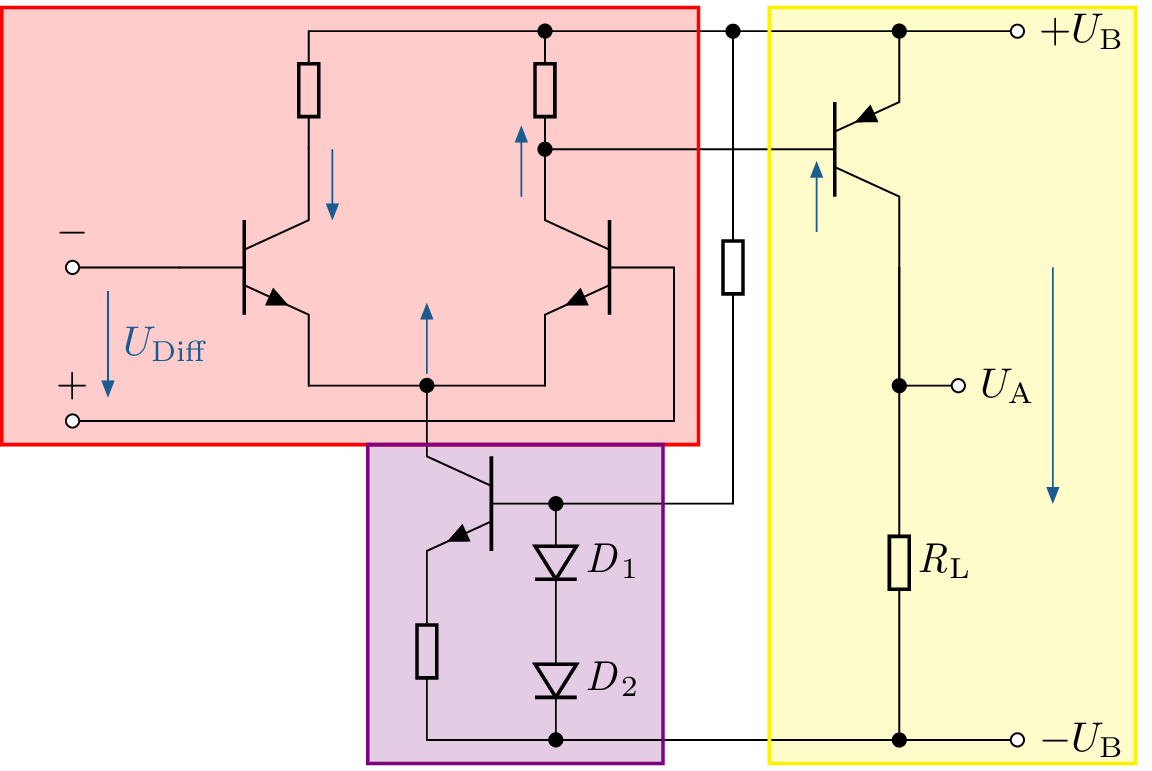
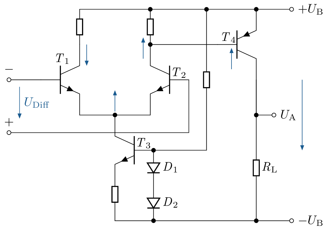
The mode of operation can be easily explained using a simplified equivalent circuit diagram (see Figure 3). This figure shows a simplified equivalent circuit diagram of an OPV made up of bipolar transistors. Today, operational amplifiers are increasingly constructed from field-effect transistors (FETs).
However, the implementation of amplifier circuits with FETs is very similar to that with bipolar transistors, which is why the mode of operation is shown here using one type of transistor. The NPN transistors \(T_1\) and \(T_2\) are identical and form the input of the operational amplifier. The differential voltage \(U_{\text {Diff}}\) to be amplified is applied between the input marked ‘+’ and the input marked ‘-’. All currents and voltages occurring in this module can vary over time and are not designated with \(U_{\text {E/A/... .}}(t)\) but with \(U_{\text {E/A/...}}\) for clarity. The inputs are referred to as the non-inverting input ‘+’ and the inverting input ‘-’. This differential amplifier at the input of the OPV is outlined in red in Figure 3. The transistor \(T_3\) functions as a current source when connected to diodes \(D_1\) and \(D_2\). The two diodes regulate the base voltage at \(T_3\) (this part of the circuit is marked in purple).
When the non-inverted input voltage increases (A), the resistance of transistor \(T_2\) decreases. This leads to a reduction in voltage at its collector and an increase at the emitter (B). Since the base of transistor \(T_4\) is connected to the collector of \(T_2\), this causes a corresponding reduction in voltage at the base of \(T_4\) (C). As a result, the collector-emitter path of the PNP transistor \(T_4\) becomes more high-impedance, so that more current flows through the load resistor \(R_{\textnormal {L}}\) (D). This increases the voltage drop across \(R_{\textnormal {L}}\) and thus the voltage at the output \(U_{\textnormal {A}}\) (the output stage of the amplifier is marked in yellow).
If, on the other hand, the inverted input voltage increases, the resistance in the collector-emitter path of transistor \(T_1\) decreases (see Figures 4). This leads to a decrease in the voltage at the collector of \(T_1\) and a simultaneous increase at the emitter. Since the emitters of \(T_1\) and \(T_2\) are connected to each other, the voltage at the emitter of \(T_2\) also increases. This reduces the voltage difference between the base and emitter of \(T_2\), making its collector-emitter path more high-impedance. As a result, the voltage at the collector of \(T_2\) increases, which increases the base voltage of \(T_4\). This makes transistor \(T_4\) more resistive, which reduces the current flow through resistor \(R_{\text {L}}\) and consequently lowers the voltage at \(R_{\text {L}}\). The output voltage of this operational amplifier can thus be controlled between \(+U_{\text {B}}\) and \(-U_{\text {B}}\).
This circuit already reveals some important characteristics of the real operational amplifier:
Key point:

Introduction, structure and function of operational amplifiers
Modelling and characteristic variables...