Conductivity and resistance
Conductivity, or conductance \(G\), describes, as the name implies, the ability of a material to conduct electrical current. The higher the value, the better a material conducts, i.e., the easier it is for charge carriers to move within the material. This property is based on the experiments of German experimental physicist Georg Simon Ohm in the early 19th century, in which he discovered that the current is proportional to the applied voltage. The reciprocal of the conductance is the more commonly used ohmic resistance \(R\). The conductance \(G\) has the unit Siemens (S), while the ohmic resistance has the unit ohm. (\(\Omega \)).
In circuit design, the physical property of ohmic resistance is used to achieve the desired functions. Figure 1 shows different designs of electrical resistors. Regardless of the design, all ohmic resistors are based on the fundamental principles of physics, which will be discussed in more detail below.
Learning objectives: Conductivity and resistance
The Students
- are familiar with the electrical component known as a resistor.
- can explain the different component designs of resistors.
- can perform calculations using the specific resistance \(\rho \) or the specific conductance \(\kappa \).
- can analyse the differences in conductivity of various materials based on their atomic structure and temperature.
1 Electrical conductivity
The definition of current density \(J\) and current \(I\) is known from Module 1. Substituting formulas 2 and 3 into formula 1 yields formula 4: \begin {equation} J=\frac {\Delta I}{\Delta A} \end {equation} \begin {equation} I = \frac {\Delta Q}{\Delta t} \end {equation} \begin {equation} \Delta V=\Delta A \cdot \Delta x \Leftrightarrow \Delta A = \frac {\Delta V}{\Delta x} \end {equation} \begin {equation} J=\frac {\Delta Q \cdot \Delta x }{\Delta t \cdot \Delta V} \end {equation}
2 Electrical conductivity
By inserting the drift velocity \(v_{el}\) and the space charge density \(\rho \) known from Module 1 into Formula 4, Formula 7 for the current density is obtained. \begin {equation} v_{el}=\frac {\Delta x}{\Delta t} \end {equation} \begin {equation} \rho = \frac {\Delta x}{\Delta V} \end {equation} \begin {equation} \vec {J}=\rho \cdot \vec {v_{el}} \end {equation} Since velocity always has a magnitude and a direction, current density is also a vector.
3 Electrical conductivity
The drift velocity \(\vec {v_{el}}\) of the free charge carriers is proportional to the electric field \(\vec {E}\), but in the opposite direction. The proportionality factor is also referred to as electron mobility \(\mu _e\). \begin {equation} \vec {v_{el}}=- \mu _e \cdot \vec {E} \end {equation} The space charge density \(\rho \) is composed of the elementary charge \(e^-\) and the charge carrier density \(n_e\). Due to the negative charge of electrons, this results in a negative sign. \begin {equation} \rho = - n_e \cdot e^- \end {equation} Substituting \(\vec {v_{el}}\) and \(\rho \) into formula 7 yields the following expression: \begin {equation} \vec {J} = (-n_e \cdot e^-) \cdot (-\mu _e \cdot \vec {E}) \end {equation}
4 Electrical conductivity
The minus signs cancel each other out, resulting in the following formula for the current density \(\vec {J}\): \begin {equation} \vec {J}=n_e \cdot \mu _e \cdot e^- \vec {E} \end {equation} The material-dependent components \(n_e\) and \(\mu _e\) as well as the natural constant \(e^-\) multiplied together yield the specific conductivity \(\kappa \): \begin {equation} \kappa = n_e \cdot \mu _e \cdot e^- \end {equation} In summary, this description results in the description of Ohm’s law: \begin {equation} \vec {J}=\kappa \cdot \vec {E} \leftrightarrow \vec {E}=\frac {\vec {J}}{\kappa } \end {equation}
\begin {equation} U_{12}=\int _{P_1}^{P_2} \vec {E} \mathrm {d}\vec {s} \end {equation} Since the electric field runs parallel to the length of the conductor, the scalar product is: \begin {equation} U_{12}=\int _{x=0}^{x=l} \vec {E} \mathrm {d}\vec {x} \end {equation} By substituting the rearranged formula 13 into \(\vec {E}\), the following follows: \begin {equation} U_{12}=\int _{0}^{l} \frac {J}{\kappa } \mathrm {d}x \end {equation}
Since it is a homogeneous material, \(\kappa \) is constant. \begin {equation} U_{12}=\frac {1}{\kappa }\cdot \int _{0}^{l} J \mathrm {d}x \end {equation}
The following formula for current density \(J\) is known from Module 1: \begin {equation} J=\frac {I}{A} \end {equation} Inserting the formula yields the following expression: \begin {equation} U_{12}=\frac {1}{\kappa }\cdot \int _{0}^{l} \frac {I}{A} \mathrm {d}x \end {equation}
Electrical conductivity indicates how well a material can transport charge carriers, i.e. how well electrical current flows through it. Materials with very good conductivity are called conductors (in extreme cases also superconductors), while materials with very poor conductivity are called insulators. Conductive media include metals such as copper, silver, aluminium and gold, which are most commonly used in electrical engineering. Insulators include plastics (polyethylene (PE), polytetrafluoroethylene (PTFE or Teflon), polyvinyl chloride (PVC), etc.), mineral oils, silicones and epoxy resin (e.g. as casting compound) specially manufactured for use as insulators, or even paper. There are also semiconductors such as silicon and germanium, whose conductivity falls between that of conductors and insulators. Their conductivity can be altered by doping and external influences such as temperature and light. These properties are used in components such as diodes or transistors to perform certain functions. The different types and properties of semiconductors are very extensive and will be covered in later modules. For the sake of completeness, it should be mentioned that liquid media such as acids or salt solutions are conductive and are referred to as electrolytes. There are also ionised gases that contain freely moving charge carriers and can conduct electric currents. These conductive gases are called plasmas, which are also not covered in this module.
5 Drift behaviour of electrons in conductors
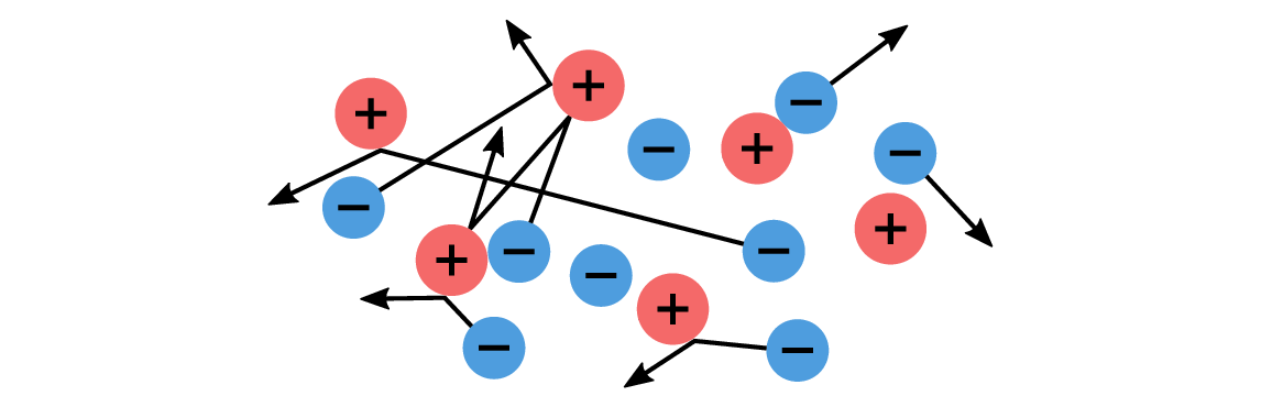
In Module 1, we already learned that electric current flow is the directed movement of free charge carriers. In the case of a conductor, these are the negative charge carriers, i.e. the electrons, which can move freely within the material. The structure of such a material consists of a solid lattice of atomic nuclei and freely moving electrons. Both the mobility of the electrons \(\mu _{\mathrm {e}}\) and their number depend on the material. In a field-free space, these electrons move randomly in all directions, resulting in a neutral state. Since this is not a directed movement but one that is evenly distributed in all directions, no current flow can be detected. Nevertheless, this undirected, temperature-dependent movement of the charge carriers leads to electrotechnical effects: In sensitive circuits, it is perceived as noise. The free charge carriers are much lighter than the atomic nuclei anchored in the lattice, so that when a moving electron collides with an atomic nucleus, an inelastic collision occurs and the direction of motion of the electron changes. This behaviour can be seen in Figure 2.
As soon as a conductor is placed in an electric field, the Coulomb force acts on the electrons, causing their
random direction of movement to change into a directed movement that points in the opposite direction to
the field (Abb.3). This directed movement of the charge carriers is referred to as current flow (see Module 1)
. However, collisions with the atomic nuclei continue to occur. These ultimately lead to a weakening of the
directional motion and thus of the current (see Fig. 3). As the atomic nuclei move more rapidly with
increasing temperature, the probability of collisions between the electrons and the nuclei increases with
increasing temperature.
This behaviour of electrons is also called drift behaviour, which depends heavily on the material. Since the atomic composition depends on the material, the number of free electrons and their mobility \(\mu _{\mathrm {e}}\) also differ. These two properties are summarised under the term specific conductivity \(\kappa \). The specific conductivity can thus be used to determine the drift velocity of the electrons in the lattice structure of the conductor. The following section deals with these properties.
6 Mathematical relationships of conductivity
The different atomic compositions of the materials result in material-dependent electrical conductivity. The material-specific properties consist of the specific conductivity \(\kappa \) (kappa) or the specific resistance \(\rho _\mathrm {R}\) (rho), which are inversely proportional to each other, as well as the respective temperature coefficient \(\alpha \), which differs depending on the material.
\begin {equation*} [\kappa ] = 1\,\, \frac {\text {Siemens}}{\text {m}} = 1\,\, \frac {\text {S}}{\text {m}} = 1\,\, \frac {\text {1}}{\Omega \cdot \text {m}} \end {equation*} \begin {equation} \kappa = \frac {1}{\rho _\mathrm {R}} \end {equation}
\begin {equation} \rho _\mathrm {R} = \rho _\mathrm {{20^\circ C}} \cdot (1 + \alpha (\vartheta - 20\mathrm {^\circ C})) \end {equation} The temperature of the conductor is entered for \(\vartheta \) (theta). This results in (\(\vartheta - 20^\circ C\)), which is the temperature difference between the actual temperature of the conductor and the \(\mathrm {20^\circ C}\) at which the reference value was determined. If \(20^\circ C\) is used for \(\vartheta \) (theta), \(\alpha \) is also omitted and the reference value \(\rho _\mathrm {20^\circ C}\) remains. The following table shows examples of some materials with their specific properties:
| Material | Specific conductivity [\(\kappa \)] = S/m | Temperature coefficient [\(\alpha \)] = 1/K |
| Silver | \(6.1\cdot 10^{7}\) | 0.0038 |
| Copper | \(5.8 \cdot 10^{7}\) | 0.0038 |
| Gold | \(4.5 \cdot 10^{7}\) | 0.0034 |
| Aluminium | \(3.7 \cdot 10^{7}\) | 0.004 |
| Iron | \(1.0 \cdot 10^{7}\) | 0.0065 |
| Graphite | \(3 \cdot 10^{6}\) | -0.0002 |
| Silicon (doped) | \(1 - 10^6\) | -0.075 |
| Tap water | \(5.0 \cdot 10^{-3}\) | - |
| Air | \(4.0 \cdot 10^{-15}\) | - |
Equivalent to the specific conductivity \(\kappa \) and the specific resistance \(\rho _\mathrm {R}\), the corresponding resistance \(R\) or conductance \(G\) of a body can be determined.
\begin {equation*} [G] = 1\, \text {Siemens} = 1\, \text {S} = 1\,\, \frac {\text {1}}{\Omega } \end {equation*} \begin {equation} G = \frac {1}{R} \end {equation}
The electrical conductivity or resistance of a conductor is also determined by its geometric properties. Both the length \(l\) and the cross-sectional area \(A\) contribute to the conductivity or resistance value. Figure 4 shows such a conductor with its properties.
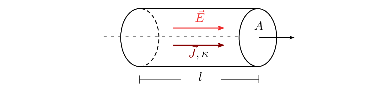
The current density \(\vec {J}\) is derived from the electric field \(\vec {E}\) and the specific conductivity \(\kappa \). The current density is independent of geometry. Only when calculating the current \(I\) must the length and cross-sectional area be taken into account. The resistance value can be calculated using the following formula:
\begin {equation*} [R] = 1\, \text {Ohm} = 1\, \text {$\Omega $} \end {equation*} \begin {equation} R = \rho _\mathrm {R} \cdot \frac {l}{A} \end {equation}
\begin {align*} \rho _\mathrm {R} & : \text {spezifischer Widerstand des Materials } (\Omega \text {m}) \\ l & : \text {Länge des Materials (m)} \\ A & : \text {Querschnittsfläche des Materials } (\text {m}^2) \\ \end {align*}
Introduction to the representation of circuits
In electrical engineering, so-called circuit diagrams are used to represent electrical networks. These circuit diagrams contain circuit symbols, which are used to represent electrical properties or entire components. Figure 5 shows an example of such a circuit diagram.
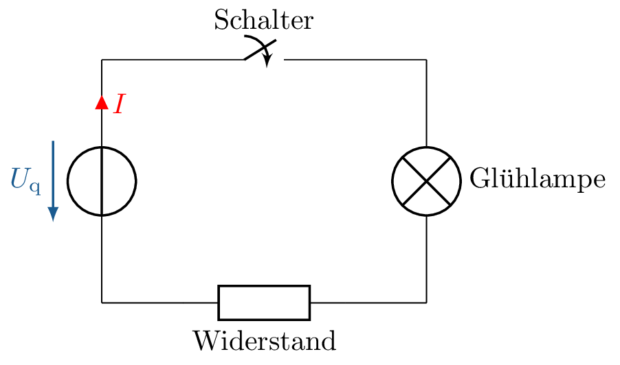
The circuit diagram consists of four elements connected by lines. It represents a series connection consisting of a voltage source, a switch, an incandescent lamp and a resistor. The resistor represents the line resistance of the entire line, while the connecting lines represent ideal connections without any other properties by definition.
Furthermore, a voltage \(U_{\mathrm {q}}\) and the current \(I\) are shown, but the current can only flow when the switch is closed. The three basic electrical properties and their circuit symbols are discussed in more detail below.
7 Resistance as a component
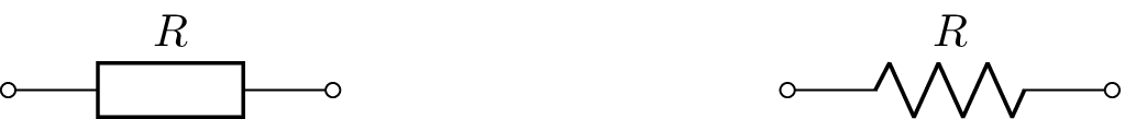
Using the method for calculating resistance described in the previous section, the resistance value of electrical cables or other conductive objects can be determined. Once a resistance value is known, it is assigned to a circuit symbol in electrical circuit diagrams. This allows different components and their properties to be connected to each other in order to determine their behaviour. Figure 6 shows two common circuit symbols for resistance.
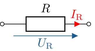
As soon as a DC voltage source is connected to a resistor \(R\), the current and voltage behave linearly. Figure 7 shows the current \(I_\mathrm {R}\) flowing through the resistor, as well as the voltage drop \(U_\mathrm {R}\).
The circuit symbol for resistance is always considered to be an ideal resistor in circuits. If temperature dependence is neglected, this is largely true in the case of direct current (except for switching operations). In reality, there are many situations in which a real resistor cannot exhibit linear behaviour. Different types of sources are discussed in sections 1.2 on voltage and current sources. To understand Figure 8, it is advisable to read sections 1.3 and 1.4 first.
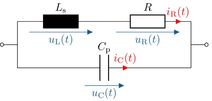
Based on the design of a resistor and the frequency at which it is operated, so-called parasitic effects become noticeable. Figure 8 shows the equivalent circuit diagram of a real resistor. If this is operated at higher frequencies, the parasitic properties (parasitics) can predominate and lead to completely different behaviour. More on this in later modules. However, complete equivalent circuit diagrams are always assumed in the following. If a resistor is only represented by its circuit symbol, it should be assumed that this is a complete description. This also applies to all components derived in the following.
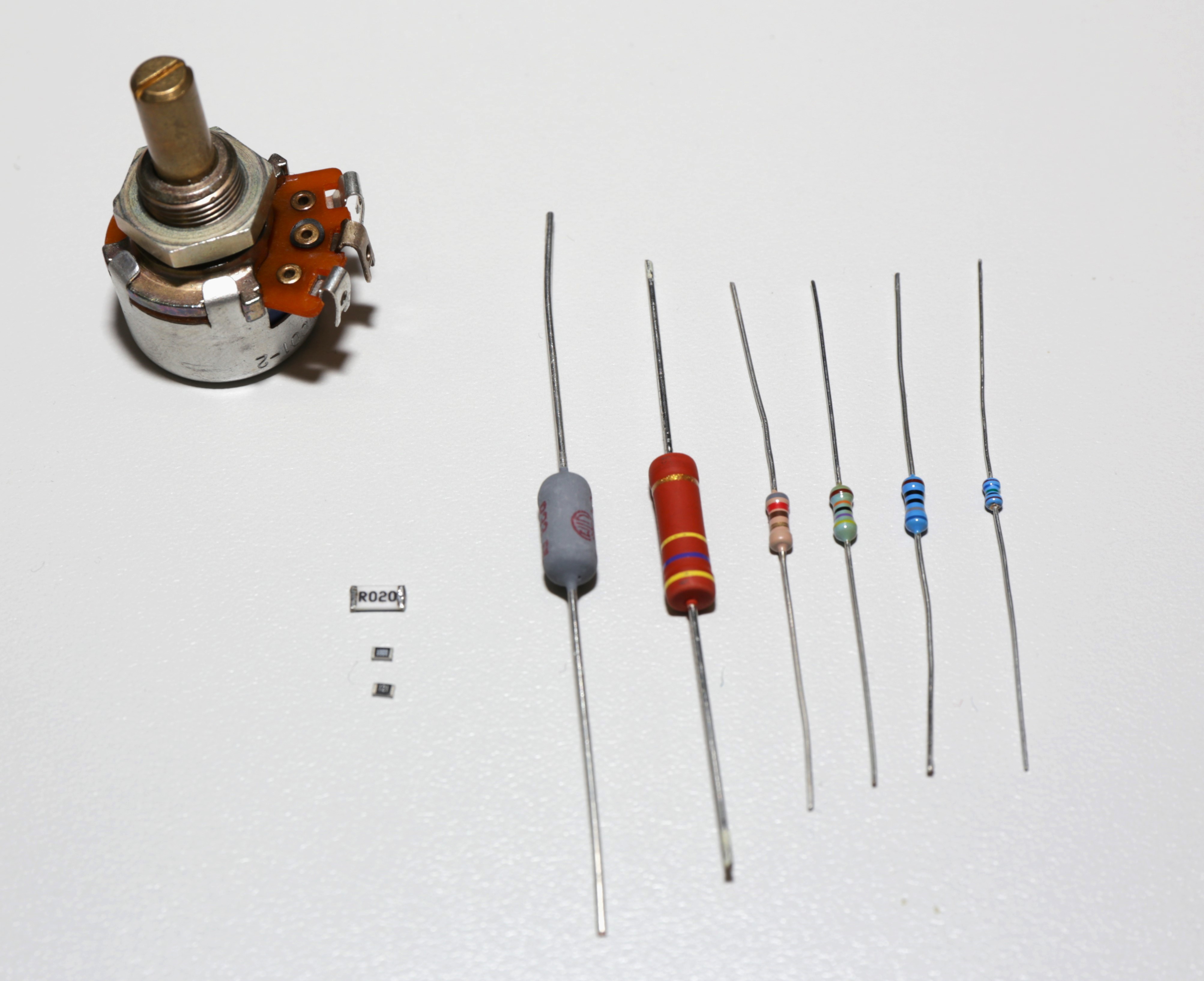
In electrical engineering, resistors, also known as fixed resistors, are used in circuit design. One of the best-known types are THT (through-hole technology) resistors. Although this type has been replaced by SMD (surface-mount device) components in many applications, there are still cases where they make sense. Examples include prototyping, DIY projects, power applications, or printed circuit boards with high mechanical requirements.
THT resistors are marked with coloured rings that provide information about the resistance value and tolerance. Figure 9 shows a THT resistor with the corresponding reading scheme and a table for reading the values:
| Colour | 1. 2. 3. Band | Multiplicator | Tolerance | ||
| Black | 0 | \(1\,\Omega \) | - | ||
| Brown | 1 | \(10\,\Omega \) | \(\pm \, 1\,\%\) | ||
| Red | 2 | \(100\,\Omega \) | \(\pm \, 2\,\%\) | ||
| Orange | 3 | \(1\,\text {k}\Omega \) | - | ||
| Yellow | 4 | \(10\,\text {k}\Omega \) | - | ||
| Green | 5 | \(100\,\text {k}\Omega \) | \(\pm \, 0.5\,\%\) | ||
| Blue | 6 | \(1\,\text {M}\Omega \) | \(\pm \, 0.25\,\%\) | ||
| Violette | 7 | \(10\,\text {M}\Omega \) | \(\pm \, 0.1\,\%\) | ||
| Grey | 8 | - | \(\pm \, 0.05\,\%\) | ||
| White | 9 | - | - | ||
| Gold | - | \(0.1\,\Omega \) | \(\pm \,5\,\%\) | ||
| Silver | - | \(0.01\,\Omega \) | \(\pm \,10\,\%\) | ||
THT resistors are available in various designs, each with their own advantages and disadvantages. Figure 10 shows four ways in which these can be implemented.

Key point:
Der Widerstandswert eines Materials hängt von seinen geometrischen und spezifischen Eigenschaften ab.
8 PTC and NTC
This section deals with a special category of resistors that are particularly useful in temperature-dependent applications: PTC and NTC resistors. The names refer to their positive and negative temperature coefficients \(\alpha \), which were already introduced in section 1.1.3. These special resistors, also known as thermistors, differ from conventional resistors in that their resistance value is highly dependent on temperature. Figure 11 shows the opposite behaviour of both types of resistance.
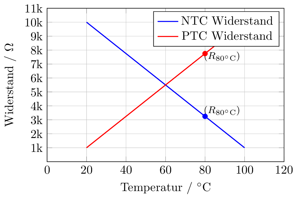
PTC resistors have a positive temperature coefficient \(\alpha \), which can be found in Table 1 in Section 1.1.3. Highly conductive materials have a positive \(\alpha \), which means that their resistance increases at higher temperatures. This makes them more conductive when cold, which is why they are also called ‘cold conductors’. Figure 12 shows the same PTC resistor at different temperatures.
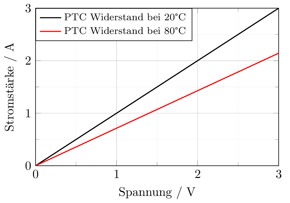
The following diagram shows the heating of a PTC resistor when the current flow increases. The more current flows through a PTC resistor, the more it heats up.

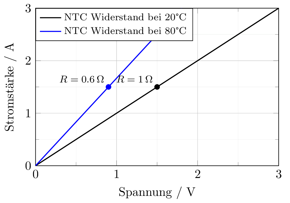
An NTC resistor exhibits the exact opposite behaviour due to its negative temperature coefficient. Typical materials with this behaviour are graphite or silicon. Since these resistors conduct better at higher temperatures, they are also called thermistors. Figure 14 shows that the resistance has a lower resistance value at a higher temperature.